
Rigaku Corporation, a global solution partner in X-ray analytical systems and a group company of Rigaku Holdings Corporation (headquarters: Akishima, Tokyo; CEO: Jun Kawakami; “Rigaku”), announced the expansion of its development of metrology technologies for next-generation semiconductors, leveraging global research environments.
This press release features multimedia. View the full release here: https://www.businesswire.com/news/home/20260512888328/en/
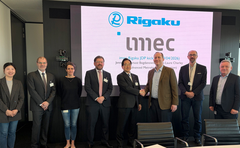
Signing ceremony with imec held on April 9
As part of this initiative, Rigaku is working with imec, a world-leading semiconductor research and innovation hub headquartered in Belgium, under a three-year development program. Through this effort, Rigaku will advance its core X-ray technologies, including 3D device metrology, high-sensitivity detection of ultrathin films and trace elements, and non-destructive inspection of microscopic defects.
As semiconductor devices evolve toward advanced architectures such as Gate-All-Around (GAA) and Complementary FET (CFET)1, along with increasing memory density, manufacturing processes are becoming more complex. These drives growing demand for highly accurate, non-destructive measurement and inspection technologies to support stable mass production. Rigaku addresses these needs by delivering high-value, differentiated metrology and inspection solutions.
Key focus areas
- Advanced logic: Metrology and inspection technologies for CFET devices
- Reticle metrology: Evaluation of photomask degradation used in EUV2 lithography
- Advanced wiring and packaging3: Non-destructive inspection technologies
- Advanced memory: Evaluation of nanostructures in 3D DRAM (a next generation memory device)
Markus Kuhn, Executive Officer and General Manager of Semiconductor Metrology Division of Rigaku, commented, “The serviceable available market (SAM) for Rigaku’s metrology and inspection products in the advanced AI semiconductors is expected to reach approximately US$1 billion by 2030. To address this market growth, Rigaku will continue introducing high‑value, differentiated products, with the goal of achieving a 50% share of this SAM. Strengthening our collaboration with imec will further enhance our competitiveness in high value-added measurement and inspection, supporting medium- to long-term growth.”
1 GAA/CFET: Gate-All-Around / Complementary Field-Effect Transistors. A next-generation device architecture in which n-type and p-type transistors are vertically stacked to increase device density beyond nanosheet (GAA) technology.
2 EUV exposure: A core technology for advanced semiconductor manufacturing that enables the formation of ultrafine circuit patterns.
3 Advanced packaging: Packaging technologies that integrate multiple semiconductor chips to enhance performance and reduce power consumption
About the Rigaku Group
Since its establishment in 1951, the engineering professionals of the Rigaku group have been dedicated to benefiting society with leading-edge technologies, notably including its core fields of X-ray and thermal analysis. With a market presence in 136 countries and regions and some 2,000 employees from 9 global operations, Rigaku is a solution partner in industry and research analysis institutes. Our overseas sales ratio has reached approximately 70% while sustaining an exceptionally high market share in Japan. Together with our customers, we continue to develop and grow. As applications expand from semiconductors, electronic materials, batteries, environment, resources, energy, life science to other high-tech fields, Rigaku realizes innovations “To Improve Our World by Powering New Perspectives.”
For details, please visit: rigaku-holdings.com/english
View source version on businesswire.com: https://www.businesswire.com/news/home/20260512888328/en/
© Business Wire, Inc.
Haftungsausschluss :
Diese Pressemitteilung ist kein von AFP erstelltes Dokument. AFP übernimmt keine Verantwortung für ihren Inhalt. Bei Fragen wenden Sie sich bitte an die im Text der Pressemitteilung genannten Kontaktpersonen/Stellen.